
India unveils indigenous PECVD system for amorphous silicon solar cell
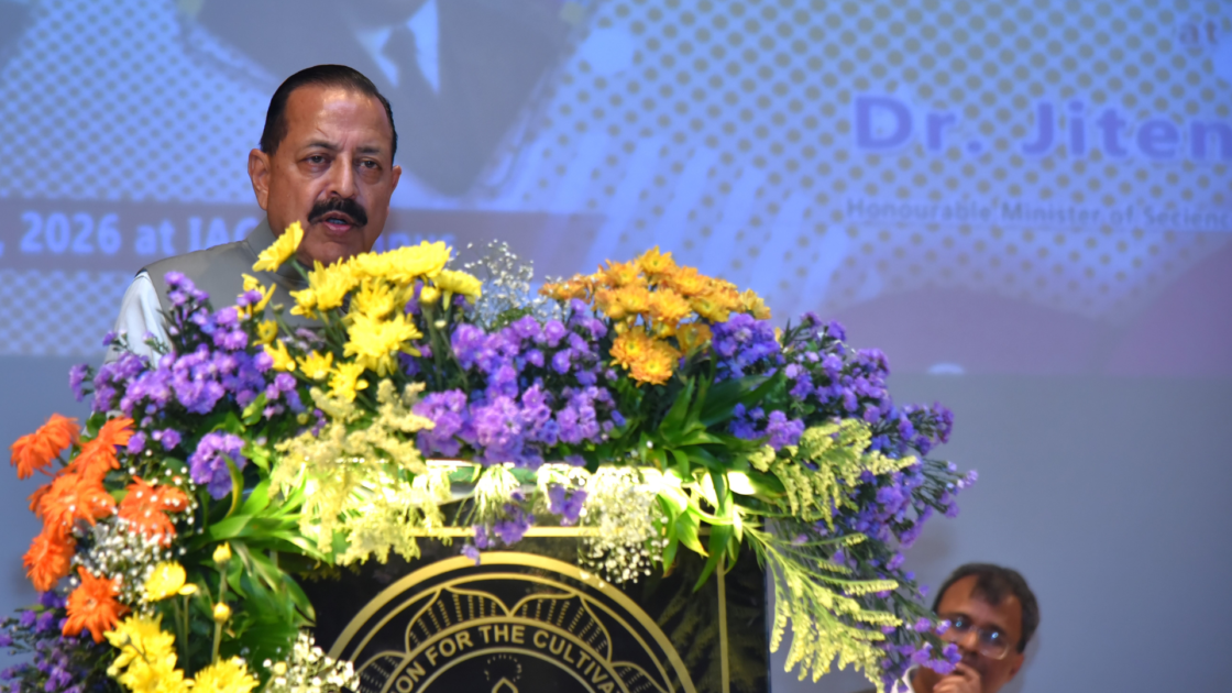
Union Minister Jitendra Singh has inaugurated an indigenously developed Plasma Enhanced Chemical Vapour Deposition (PECVD) system designed to fabricate India’s first amorphous silicon solar cell. The minister described the development as a major step toward scientific self-reliance under the Atmanirbhar Bharat initiative.
The inauguration took place during the 150th anniversary celebrations of Indian Association for the Cultivation of Science in Kolkata. Established in 1876 by Mahendralal Sircar, the institution is recognised as India’s first research centre founded by Indians for modern scientific research.
The institute is also known as the birthplace of the Raman Effect, discovered by Nobel laureate C V Raman.
PECVD technology
PECVD is a thin-film deposition process widely used in solar cell manufacturing. The technology enables deposition of high-quality thin layers such as silicon nitride (SiN) and silicon dioxide at relatively low temperatures.
These layers function as anti-reflective coatings to improve light absorption and as passivation layers to minimise electrical defects in solar cells.
Under the process, gases are introduced into a vacuum chamber and converted into plasma using electromagnetic energy such as radio frequency or microwaves. The plasma chemically transforms the gases, resulting in uniform deposition of thin-film material on the solar cell substrate.
Since the plasma drives the chemical reaction, PECVD can operate at significantly lower temperatures than conventional chemical vapour deposition methods, helping prevent damage to silicon wafers.
According to Singh, the new facility strengthens India’s indigenous renewable energy research and technological capabilities.
RETINA incubation centre
The minister also inaugurated RETINA — Research Entrepreneurship for Translation, Innovation and Navigation — an incubation centre intended to support commercialisation of scientific research and promote startup-driven innovation.
Singh said Indian scientific institutions are increasingly linking research with entrepreneurship, industrial partnerships, and practical applications in areas such as healthcare, clean energy, and sustainable development.
Emerging research areas
The minister noted that IACS has produced several prominent scientific figures, including Satyendra Nath Bose, and continues to contribute to research in physical sciences, biological sciences, materials science, and interdisciplinary technologies.
He also highlighted the institute’s work in areas including quantum materials, nanotechnology, artificial intelligence, battery materials, cancer biology, and environmental technologies.
Photo credit: PIB